www.kingfordpcb.com
Printed Circuit Board Layout: PCB Assembly Manufacturer in China
Printed Circuit Board Layout: PCB Assembly Manufacturer in China
Our company provides services for the design of printed circuit boards for your projects. Our experience in the design and manufacture of various types of printed circuit boards allows us to provide services for the development and tracing of printed circuit boards of any complexity and accuracy class.
We can also offer you services for the rapid design of printed circuit boards for complex tasks. When designing complex boards, we use a multi-user development mode – several PCB designers are working on a project in parallel.
What do we offer?
• Design of various types of printed circuit boards
• Analog, digital, high frequency
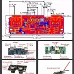
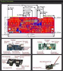
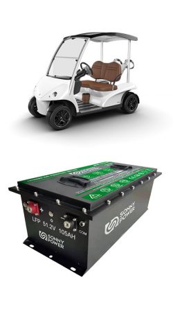
• Single and double layer printed circuit boards
• Multilayer PCB with BGA packages, with buried and blind via
• Analysis and modeling
• Compliance with DFM, DFA, DFT standards and international IPC standards
Results of PCB design service
After the completion of the project for the development of the board, the customer receives all the materials, including design documentation (CD) for the start of serial production:
• Project file corresponding to the selected design environment
• Files for PCB production
• CD for a printed circuit board, including an assembly drawing, specification and board drawing – in accordance with IPC standards, the unified system for design documentation (ESKD) or in accordance with customer requirements
Development of printed circuit boards according to DFM, DFA, DFT requirements: advantages
• Reducing the cost of manufacturing and assembling boards
• Reduced production time
• Increased quality in serial production
• Reliability of the board and an increase in the yield of suitable boards in mass production
• Testability of boards for ICT and JTAG testing
Get Best PCB Layout Manufacturer Now
Stages of PCB development
The PCB design process takes place in several stages. During the entire development cycle,international IPC standards, requirements for testing (DFT), manufacturing (DFM) and assembly (DFA) are taken into account, the thermal mode of the device is analyzed.
How does PCB Layout Process take place?
PCB design is a mechanical and electrical design process. In the process of developing a printed circuit board, electrical elements are connected with conductive circuits, but the process of connecting elements is actually one of the most recent stages of designing a board and is mostly denoted by the term – routing.
Initially, it is required to analyze and the possibility of placing the elements of the electrical circuit on the surfaces of the board in the given overall dimensions, which are usually determined by the design features of the entire product and, in particular, by the product body.
Upon completion of the placement stage, the electrical elements are combined. In the process of connecting electrical elements, it is necessary to take into account many parameters, such as the magnitude of the current, characteristic impedance, the influence of adjacent electrical circuits, etc.
PCB design:
• placement of elements on the area indicated in the terms of reference;
• preparation of a layout 3D model;
• coordination of placement with the Customer on the 3D model;
• conducting routes between elements in accordance with the developed circuit design;
• simulation of the resulting structure for compliance with the requirements of signal integrity, for compliance with the requirements for the power supply system, for compliance with the requirements of electro-magnetic compatibility, for compliance with the requirements of temperature distribution;
• preparation of the final 3D model;
• coordination of the received design with the Customer according to the 3D model;
• The preparation of a list of equipment for the purchase of elements;
• preparation of gerber files for the production of printed circuit boards;
• Preparation of files for installation work.
Get PCB Layout Service Quote
Best PCB Fabrication design center
We present a design center for the development of printed circuit boards according to the electrical diagram provided by the customer. We perform PCB tracing, modeling and preparation of production files.
We understand perfectly understand how to wire high-speed signals, sensitive analog signals, microwave signals, how to arrange ground and power polygons, how to connect filter capacitors to high-power microcircuits.
Extensive Experience in High Quality PCB Layout Services
Often, our specialists, on the basis of their many years of experience, even suggest to a schematic designer where potential problems may be present in his circuit, or how best to perform this or that part of the routing or placement of components on the board.
This gives customers serious advantages over their competitors:
• Improved quality of production and assembly of printed circuit boards.
• Reducing the time from development to the final product (time-to-market).
• No errors due to the definition of a library of components for each company separately.
• Provision of guarantees for the compliance of the printed circuit board with the requirements of the technical task.
• Close interaction with the customer throughout the entire design process.
• Accurate design – fewer iterations and cost savings.
PCB Board- Backbone of Electronics Industry
https://www.kingfordpcb.com/
A printed circuit board is one of the structural elements of any modern electronic device. It is primarily intended for mechanical fixation and electrical connection of electrical circuit elements of an electronic device.
Structurally, a printed circuit board is a plate made of a dielectric material (in most cases, but it is possible to use structures on an aluminum substrate to improve heat dissipation) with electric circuits formed on its surface and volume.
Features of our PCB Layout Center
There is an opinion that the work on designing a printed circuit board cannot be given to a subcontractor, because it is very difficult to prepare a technical assignment, make a full-fledged scheme and interact with the designer “remotely”. Perhaps this really often happens when working with “freelancers”, third-party developers, and sometimes employees of their own company.
Get instant Quote to execute your Future PCB Project
However, the experience of our design bureau shows that in this case this opinion does not correspond to reality. Companies that turn to a design center with design orders actually significantly increase their efficiency, significantly improve the quality and increase the speed of project execution, and hence the number of projects completed per year.