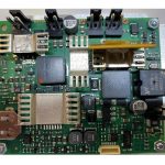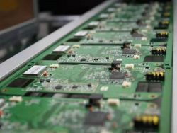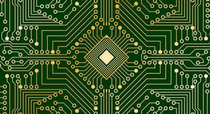
PCB Fabrication
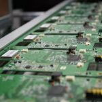
Printed circuit board (PCB) fabrication is a method of assembling circuit boards used in computers and other electronic products in which the various layers of the circuit board are combined together with a specific surface pattern so that it can be used for electronic manufacturing. As the one of PCB fabrication companies in China, HX can manufacture PCB in-house or outsource it to an company that specializes in manufacturing.
Features of PCB Fabrication
Printed circuit board (PCB) fabrication is a method of assembling circuit boards used in computers and other electronic products. The layers of a circuit board are put together along with a specific surface pattern so that it can be used for electronics manufacturing. PCB fabrication companies can manufacture PCBs in-house or outsource this aspect of production to a specialist. PCB fabrication process begins with design. Some PCB fabrication specialists can also design the board, using specifications provided by the customer.
In other cases, customers develop their own files and send them to the PCB fabrication manufacturers. These files are presented in a format called Gerber file, an industry standard for recording PCB-specific details. PCB fabrication companies use Gerber files to program PCB manufacturing for their devices. A variety of techniques can be used, depending on the need for production. Custom products tend to be more expensive because they require small production runs, while generic or standard formats are less costly.
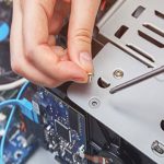
Prototypes, produced in very limited quantities of boards, can be very expensive. And in some cases, to limit PCB fabrication cost and reduce the loss of proprietary information, the conductive foil layers are glued together before being covered with solder masks This is the basis for connecting the thin copper wires of the circuit and can be done by plating or other means. Multiple layers can be made using certain PCB fabrication methods. The finished PCB is assembled with other components and tested to confirm that it works properly before being sent to the customer.
PCB Fabrication Process
The PCB fabrication is a complex process that begins with a product concept and ends with a fully functional PCBA. Here is a sequence of steps of the PCB fabrication process, total of eight steps, generated by PCB fabrication companies.
Step 1 – The Design.
Step 2 – Printing the Design.
Step 3 – Creating the Substrate.
Step 4 – Printing the Inner Layers.
Step 5 – Ultraviolet Light.
Step 6 – Removing Unwanted Copper.
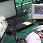
Step 7 – Inspection.
Step 8 – Laminating the Layers.