Semiconductor industry Sputtering Targets
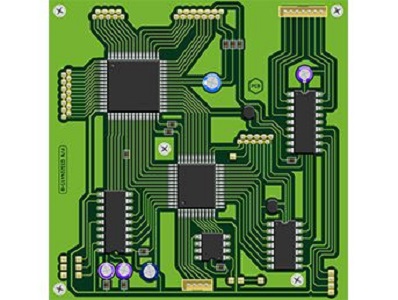
Sputtering targets are used in wafer fabrication and chip packaging. In wafer fabrication, targets are mainly used to make conductive layers, barrier layers, and metal gates.
In the chip packaging link, the target is used to generate metal layers, wiring layers and other metal materials under the convex points. Although the amount of target material in the field of wafer fabrication and chip packaging is not large, accounting for only 3%, but the quality of the sputtering target for Semiconductor industry directly affects the uniformity and performance of the conductive layer and barrier layer, and then affects the transmission speed and stability of the chip. Therefore, target material is one of the core raw materials of semiconductor production.
Covering Logic IC, power IC, DRAM, LED, discrete device and more.
Provide all kinds of metal / non-metal high purity sputtering target materials (Al, Cu, Ti, Ta ,W, Au, Ag).