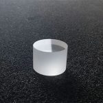
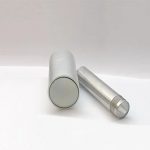
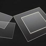
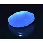
Ce YAP Substrates
Ce:YAP is a fast scintillation crystal with excellent performance. It has high light output, fast decay time, good thermal stability and mechanical properties, and stable chemical properties. Ce:YAP scintillation crystals are mainly used in fast gamma-ray detection, animal PET scanning systems, electronic imaging (SEM), high-energy physics, low- and medium-energy X-ray two-dimensional imaging and other fields.
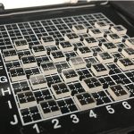
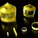
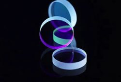
OST Photonics offers high quality Ce:YAP substrates for researchers and industries. Crystal size and thickness can be customized according to your requirements.
Application of Ce YAP Substrates
Gamma, X-ray counter
X-ray imaging screens
Electron imaging screens
Ion beam imaging
Scanning electron microscope(SEM)
Advantages of Ce YAP Substrates
High density
Stable physical and chemical properties
Fast decay time
No hygrscopic
No cleavage planes
High temperature resistance
Ability of Ce YAP Substrates
Maximum Size: ɸ50mm x 160mm
Dimension: 1”, 25x25mm, 10x10mm, 10x5mm, 5x5mm, etc.
Thickness: 0.5mm, 1.0mm, etc.
Available items: substrate, blanks, scintillation screen and customized optics
Specification and properties of Ce YAP Substrates
Crystal System
Orthogonal
Density
5.4 g/cm3
Hardness
8.5 Mohs
Melt Point
1875 ℃
Effective Atomic Number
39
Peak Wavelength
370 nm
Refractive index at peak emission
1.95
Cleavage
No
Deliquescence
No
Decay Time
28 ns
Light Yield
25 photons/KeV
Radiation Length
2.7 cm
Dimension
1”, 25x25mm, 10x10mm, 10x5mm, 5x5mm, etc.
Dimension Tolerance
±0.1 mm or better
Thickness
0.5mm, 1.0mm, etc.
Thickness Tolerance
±0.05 mm or better
Surface Roughness
Ra<5Å
Surface Finish
Single side polished (SSP)/Double sides polished (DSP)
Package
Class 100 clean bag, Class 1000 super clean room